💬 WhatsApp Chat

Fine Blanking for Electronics Connectors

Connector terminals, contact pins, and EMI shielding cans — fine blanking delivers burr-free edges at 0.1 mm feature sizes for high-density electronics.

Micro-Precision

Your Smartphone Has 40+ Fine-Blanked Contacts — Each One Thinner Than a Human Hair

Inside every smartphone, laptop and wearable device, there are dozens of fine-blanked electronic components: connector terminals in phosphor bronze, contact pin arrays in beryllium copper, EMI shielding cans in SUS304 stainless, and lead frames in copper alloy. These components share a common requirement that only fine blanking can satisfy: burr-free edges at feature sizes down to 0.1 mm, produced at 60-120 strokes per minute for the multi-million-unit volumes that consumer electronics manufacturing demands.

The burr-free requirement is absolute in electronics. A micro-burr on a connector terminal causes insertion damage to the mating connector, degrading contact resistance over the product's lifecycle. A burr on an EMI shielding can creates a gap in the shielding perimeter, allowing electromagnetic leakage that fails FCC and CE compliance testing. A burr on a contact pin array prevents proper seating in the PCB via, causing intermittent connections that are the most common failure mode in consumer electronics assembly.

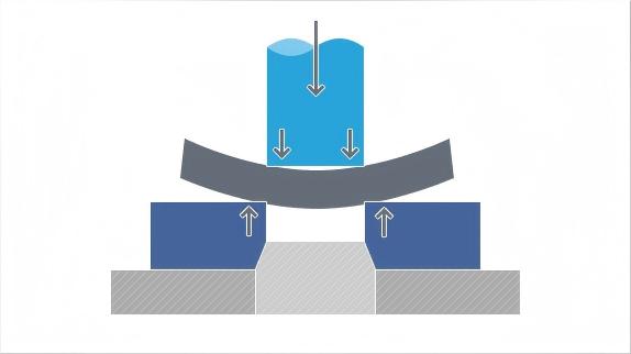
Fine blanking eliminates burrs entirely because the triple-force hydraulic system — V-ring impingement, counter-pressure and blanking force — maintains the material in compression throughout the shear zone. The resulting edge is 100% burnished with no fracture zone and no burr, ready for plating and assembly without secondary deburring. HS-FINEB's HF-200 and HF-320 presses are engineered for this precision-over-force application, where dimensional accuracy and burr-free edges matter more than tonnage.

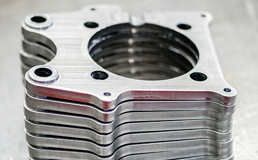
Fine-blanked electronic connector terminals and precision contacts
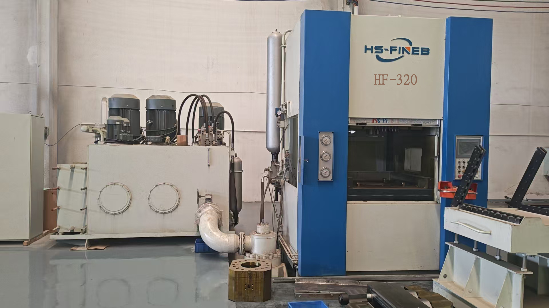
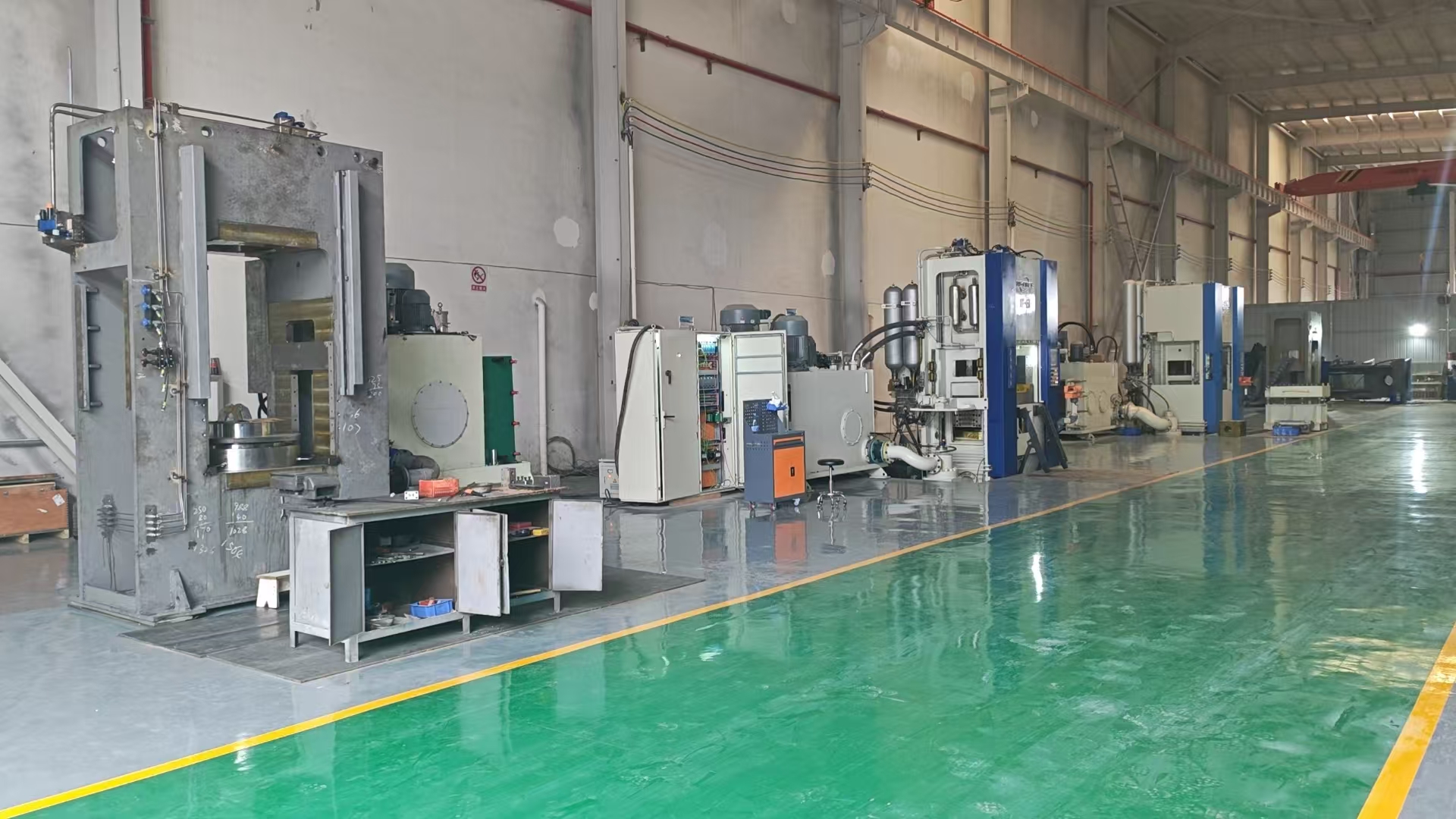
HF-320 fine blanking press for connector terminal production
Feature Size Precision

Connector Terminal Geometry: 0.1-0.3 mm Features at 0.5 mm Pitch

Modern electronic connectors push the boundaries of stamping technology. A typical USB-C connector terminal has contact beams 0.2 mm wide, spaced at 0.5 mm pitch, with a beam length of 3.5 mm and a contact radius of 0.15 mm at the beam tip. The terminal material — C5191 phosphor bronze at 0.2-0.3 mm thickness — must be blanked with 0.002 mm die clearance to maintain the beam geometry without distortion, and the 100% shear zone on the beam sidewall is essential for proper contact spring function.

Conventional progressive-die stamping of these terminals leaves a burr on the beam sidewall that varies from 0.01 to 0.03 mm across the die life, creating inconsistent insertion forces and contact resistance. Fine blanking eliminates this variability: the carbide punch with wire-EDM ground beam cavities produces identical beam geometry for the full die life, with 100% shear zone on all beam surfaces. The V-ring — miniature geometry at 0.1 mm depth and 0.2 mm distance from the beam profile — compresses the thin phosphor bronze material into the beam cavity, preventing the lateral flow that would distort the beam width.

The HF-320 with 3200 kN total force, programmable blanking speed of 5-45 mm/s, and ±0.1 mm feed pitch accuracy is the production standard for connector terminal manufacturing. The programmable speed is critical for phosphor bronze — too fast and the material work-hardens excessively at the shear zone, reducing beam flexibility; too slow and production rate drops below the economic threshold.

Single-Stroke Pin Arrays

Contact Pin Arrays: Coining and Blanking in One Stroke

Contact pin arrays — the grid of pins on a CPU socket, memory module connector or board-to-board connector — demand simultaneous formation of the pin profile, the pin tip geometry and the connecting web in a single press stroke. The pins are typically 0.3-0.5 mm in diameter, spaced at 0.5-1.0 mm pitch, and blanked from beryllium copper C17200 or phosphor bronze C5191 at 0.3-0.5 mm thickness.

Fine blanking produces these arrays using a compound die that combines coining (compressing the pin tip to form the contact radius) and blanking (shearing the pin profile from the strip) in one stroke. The V-ring surrounds each pin cavity, compressing material into the pin profile to achieve 100% shear zone on the pin sidewall — critical for the insertion-withdrawal cycle that the pin must survive. The counter-pressure pad holds the strip flat during the coining operation, preventing the web distortion that would misalign the pin array relative to the PCB via pattern.

Beryllium copper C17200 is the premium contact material for high-cycle pin arrays — 1,000+ insertion cycles with stable contact resistance — but requires careful fine blanking parameter control. The material's high yield strength (1035-1200 MPa in the age-hardened condition) requires full V-ring force even at 0.3 mm thickness, and the carbide die life is shorter than on phosphor bronze (200,000-400,000 strokes vs. 1,000,000+ strokes) due to the material's abrasiveness.

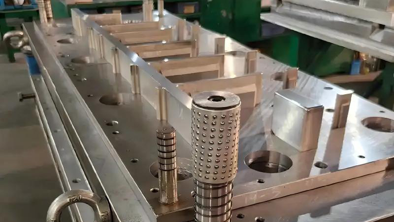
Fine blanking die for contact pin array production
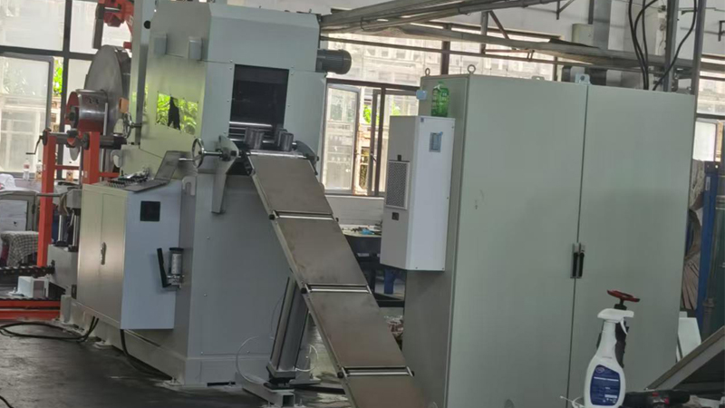
Coil feeding and leveling system for electronics fine blanking
Shield Perimeter Integrity

EMI Shielding Cans: Depth-to-Width Ratio and Spring-Back Control

EMI shielding cans are stamped metal enclosures that sit over sensitive electronic components on the PCB, creating a Faraday cage that blocks electromagnetic interference. The typical shield is a drawn or formed box, 10-40 mm on each side, 3-8 mm deep, blanked from SUS304 stainless steel at 0.2-0.4 mm thickness. The critical fine blanking requirement is on the shield's base flange — the flat perimeter that solders to the PCB — which must be burr-free to ensure continuous shielding contact with the ground plane.

A gap in the shield perimeter — caused by a burr that prevents the flange from seating flatly on the PCB — creates an antenna aperture that radiates electromagnetic energy at the gap frequency. Fine blanking eliminates this risk by producing a 100% shear zone on the flange perimeter with zero burr. The counter-pressure pad holds the thin stainless flat during blanking, preventing the spring-back that distorts the flange flatness in conventional stamping, where the unsupported strip warps as the profile is cut.

For SUS304 at 0.2-0.4 mm thickness, the HF-200 provides sufficient force for shield production, but the press must be configured with reduced V-ring depth (0.1-0.15 mm vs. 0.3-0.4 mm for thicker materials) to avoid V-ring penetration through the thin material. The coil-fed progressive die configuration, combined with the automatic feeding and leveling system, delivers 80-120 SPM production rates for shield manufacturing.

Material Selection

Copper Alloys and Stainless for Electronics Fine Blanking

C5191 Phosphor Bronze

The standard material for connector terminals and contact beams. Tin-phosphorus bronze with excellent spring properties, fatigue resistance and electrical conductivity (15-20% IACS). Hardness 180-220 HV in the half-hard temper. Fine blanking achieves 100% shear zone at 0.2-0.5 mm thickness with carbide die life exceeding 1,000,000 strokes due to the material's low abrasiveness.

C2680 Brass

General-purpose copper-zinc alloy for lead frames, switch contacts and non-critical terminal applications. Lower cost than phosphor bronze, 28% IACS conductivity, hardness 90-140 HV. Fine blanking response is excellent — die-roll below 5% of material thickness, 100% shear zone at 0.3-0.8 mm thickness. Die life on C2680 can exceed 1,200,000 strokes.

SUS304 & BeCu

SUS304 stainless for EMI shielding cans (corrosion resistance, formability) and C17200 beryllium copper for high-cycle contact pins (1,000+ insertion cycles). SUS304 requires higher V-ring force due to work-hardening; BeCu demands careful parameter control but delivers premium contact performance for CPU sockets and memory connectors.

View full material processing guide →

Production Parameters

Tooling Precision, SPM & Die Life for Electronics

ComponentFeature SizeMaterialThicknessSPMDie Life (strokes)
Connector terminal0.1-0.3 mmC5191 / C26800.2-0.5 mm80-1201,000,000+
Contact pin array0.3-0.5 mm diaC5191 / BeCu0.3-0.5 mm60-100200,000-1,000,000
EMI shield can10-40 mmSUS3040.2-0.4 mm80-120500,000-800,000
Lead frame0.15-0.3 mmC2680 / C51910.2-0.4 mm100-1201,000,000+
Switch contact0.2-0.5 mmC51910.3-0.5 mm80-1201,000,000+
Note: Die life figures assume tungsten carbide tooling (K10-K20 grade for copper alloys, K30 for stainless), 0.002 mm cutting clearance for thin-gauge materials, and per-material blanking speed optimization. The 0.002 mm clearance — approximately 0.5% of 0.4 mm material thickness — requires wire-EDM punch tips with sub-micron surface finish. Contact our engineers for project-specific tooling and die life calculations for your connector geometry.
Recommended Presses

HS-FINEB Models for Electronics Production

HF-200HF-200 fine blanking press for EMI shield cans

HF-200 (200T)

Precision-over-force platform for EMI shielding cans, lead frames and switch contacts. 2000 kN total force, 70 SPM, 500×500 mm table. Carbide die life 500,000+ strokes on copper alloys.

HF-320HF-320 fine blanking press for connector terminals

HF-320 (320T)

Production standard for connector terminals and contact pin arrays. 3200 kN force, programmable blanking speed 5-45 mm/s, ±0.1 mm feed accuracy for 0.1 mm feature precision.

AuxiliaryCoil feeding and leveling system for electronics production

Feeding System

Coil feeding and leveling system matched to 80-120 SPM cycle rates, configured for thin-gauge copper alloy and stainless strip. Precision roll leveling for flat strip delivery at 0.2 mm thickness.

Post-Blanking Quality

Deburring and Cleaning for Contact Surfaces

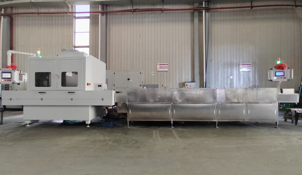
While fine blanking produces burr-free edges, the micro-deburring requirement for electronics is even more stringent than for other applications. A 0.005 mm edge radius on a connector terminal beam can affect insertion force by 15-20%, and surface contamination from stamping lubricant can degrade contact resistance. HS-FINEB provides ultrasonic cleaning and precision deburring equipment matched to the electronics production line.

The combined fine blanking + ultrasonic cleaning cell delivers terminals ready for plating — no secondary deburring, no surface contamination, no edge inspection sorting. For contact pin arrays, the cleaning process also removes the micro-burr that can form at the coining interface, ensuring 100% pin geometry compliance before the insertion-cycle validation test. Learn about our deburring and polishing equipment →

Ultrasonic deburring and cleaning equipment for electronic connector parts

Have an Electronic Component to Evaluate for Fine Blanking?

Send your part drawing, material grade and feature size requirement. Our engineers will assess the burr-free feasibility at your minimum feature size, calculate the required die clearance and V-ring geometry, and recommend the right HF-series platform for your electronics production — with carbide die life projections per material alloy.

💬